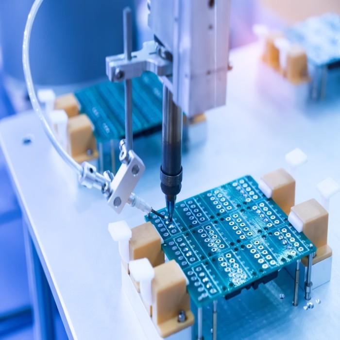
Assembly and Testing of Semiconductor Devices: Dicing and Sawing Processes

How Semiconductor Devices are Assembled and Tested
The semiconductor manufacturing process involves numerous steps to assemble and test integrated circuits (ICs) and related semiconductor devices. While the actual fabrication of semiconductors occurs at front-end fabs, assembly and testing functions are critical parts of the overall process. Let's take a deeper look at how these functions work.
Dicing and Sawing
Once wafers have been fabricated containing numerous identical ICs or die, they must be separated into individual chips. This is accomplished through dicing or sawing processes. The wafers are secured to a sticky film and a diamond-tipped saw precisely cuts narrow streets between each die on the wafer. This separation allows the individual chips to then undergo packaging and other post-fabrication processes. Sawing yields very accurate and clean cuts but can damage fragile chips. Newer laser and plasma dicing methods achieve separation without contact.
Die Attach and Wire Bonding
The next major steps are die attach and wire bonding. Semiconductor Assembly and Testing Services Die attach involves placing each separated die onto a package substrate or leadframe. An electrically conductive epoxy or solder material is used to adhere the die and provide electrical connectivity. Next, during wire bonding ultra-thin gold wires make connections between the die contact pads and the package lead terminals or substrate contacts through thermosonic or ultrasonic bonding machines. These processes build the basic electrical interconnect structure of the packaged device.
Encapsulation and Molding
After bonding, a protective encapsulation or molding material is used to encapsulate the assembled die, wire bonds and internal lead portions. Thermoplastic or thermosetting polymer compounds are typically used for molding. The package or mold is filled with the compound in semi-liquid form which then hardens around and embeds the die assembly, protecting it from environmental damage and contamination. Common molding materials include epoxy, polyester and polyimide resins suited for the required operating conditions.
External Lead Finishing
For packaged devices with external leads such as thin small-outline packages, the leads must be formed to the required shape and size configuration after the molding process. Lead frames are precision-etched from copper or alloy strip stock configured for the specific package. Post-mold lead finishing may involve mechanical stamping or bending to reshape lead profiles. In some cases, leads may also undergo secondary solder coating or plating for compatibility or reliability.
Final Testing
Comprehensive testing is performed on packaged semiconductor devices to ensure functional and parametric specifications are met before device shipment. Automated test equipment (ATE) handles high-volume electrical semiconductor assembly and testing services of key device parameters and functional operation. Tests typically include current and voltage parameter measurement at different operating conditions, input/output pin electrical verification, and full functional operations testing using automated test patterns and computer control. Any failing devices are identified and rejected to maintain product quality. Final programming or serialization may also occur, like writing codes or data to on-chip memory. Successfully tested good dies are then shipped to customers.
Outsourced Assembly and Test Services
Many fabless semiconductor companies and integrated device manufacturers outsource assembly, packaging and test operations rather than maintaining in-house assembly lines. Outsourced semiconductor assembly and test (OSAT) providers perform these downstream services as independent third-party contractors. They have specialized facilities with state-of-the-art packaging and test equipment capable of producing a wide range of device packages.
OSAT providers offer services from individual processes like die bonding or system-in-package assembly to turnkey "back-end" services encompassing all post-front-end functions from wafer probe testing through final test and shipment. Using OSATs enables fabless customers and IDMs to avoid major capital expenditure on packaging infrastructure and focus on designing new products instead. Leading OSAT companies can package and test billions of units annually giving them economies of scale advantages over maintaining in-house operations.
Key Considerations in Semiconductor Assembly and Testing Services
Several factors are important to consider when outsourcing semiconductor assembly and testing functions. Process technology capabilities and available package types are major determinants in selecting an assembly partner. Turnaround time, pricing structure, quality systems and the ability to support multiple projects simultaneously are other key criteria. Effective communication of design specs, documentation, process control and reliability are vital to achieving high yields through outsourced operations. In an increasingly complex semiconductor landscape, assembly and test services play a crucial role in taking chips from fab to the end products powering today's technologies.
Get more insights on Semiconductor Assembly And Testing Services
- Art
- Causes
- Crafts
- Dance
- Drinks
- Film
- Fitness
- Food
- Игры
- Gardening
- Health
- Главная
- Literature
- Music
- Networking
- Другое
- Party
- Religion
- Shopping
- Sports
- Theater
- Wellness


